Making Sense of Latches and Flip-Flops
I was never a good student in university. I did not care about grades, did not care about failing exams, and if for whatever reasons I was not skipping classes I was sitting in the classroom browsing Pinterest on phone, et cetera. But there's something that still bugs me till this day.
I don't actually understands how latches & flip-flops work, and - I don't know why - I couldn't stand not knowing that.
Now you may say sh*t like "ooh it's because you didn't listen in class blahblahblahblah" - I read through so many introductory texts on sequential circuits throughout this 4 years and while I kinda have an idea of how they behave I just couldn't fathom in my head why they behave in the way they behave in.
And now, I finally kinda get the hang of it.
Set-Reset Latches
Latches & flip-flops are a kind of digital circuits that can "store" stuff. It's a kind because we also have magnetic core and delay line memory and all kinds of other stuff. The simplest (okay maybe not the simplest but the most frequently mentioned in textbooks) latches is called the Set-Reset latches (abbr. SR latches), presented in the form of two intertwined NOR or NAND gates:
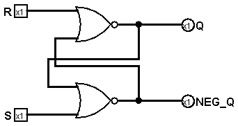
SR latch built with NOR gates
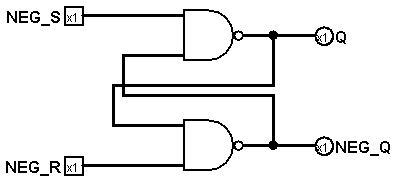
SR latch built with NAND gates
The basic idea of this kind of latches goes as follows. There's a Q signal which is the "stored" 1-bit data (Q stands for Query) and a NEG_Q signal which is the inverse of Q. If you set S to High, Q will be set to High as well, thus the bit is set; but if you set S to low after this, due to how the circuit is laid out Q will stay High, the bit of data is thus stored; the same thing goes for R, which instead of setting Q, it resets Q.
And here comes... the first bit of confusion from all the tutorial text online. Notice that in the NOR one the inputs are "S" and "R" but in the NAND one they are "NEG_S" and "NEG_R". In the NOR one S and R is "active-high" meaning it considers the signal to be "High" when it's at a higher voltage (i.e. actual high), and in the NAND one it's the opposite, meaning when it's at a lower voltage (i.e. actual low) it's considered to be on "High", so to avoid confusion people write NEG_S and NEG_R instead so they know they need to send in not the "active-low version" of S and R but the inverse of S and R. AND THEY'RE BOTH CALLED SR LATCHES! And to make things worse, some texts label the S and R signal on NAND one directly as "S" and "R"! So when you search about SR latches online you'll see people talking about two seemingly very different circuits (as in the kind of gates) but actually they're all the same (except for the active-high and active-low bit).
Some of you might look at this circuit and say, "Hold on, the output of the top gate links to one of the inputs of the bottom gate, and the output of this bottom gate becomes one of the input of the bottom gate! They depend on each other, this is not possible!" The big idea here is that this isn't math. Math does not have delay, but logic gates do, it takes time (albeit a very, very small amount of time) to produce the result, and that result takes time (albeit an even smaller amount of time) to propagate through the wiring. Taking the NOR SR latch as an example: when R=0 and S=1, the bottom gate is bound to output Low, which means NEG_Q and one of the input of the top gate would be Low; combined with R=0, the top gate outputs High, which is then propagates to Q and back to the bottom gate, everything is working correctly, all is well in the world. R=1 with S=0 is the same story but instead of resulting in Q being High it results in Q being Low.
Now, there's the second bit of confusion. If you look at the "characteristic table", it will say that R=0/S=0 is the "latch" or "hold" state, and R=1/S=1 is the "illegal" or "not allowed" state. What does this all mean? First of all, "illegal" does not mean such state isn't possible; it's illegal simply because we decided that NEG_Q must be the inverse of Q but R=1/S=1 will result in Q and NEG_Q both being 0.
As for the "latch" state things are a little bit different - it will only become the "latch" state when the input is transitioning from R=0/S=1 or R=1/S=0. If this state is directly reached from R=1/S=1 and if the delay of the two gates are exactly the same, it will end in a state called the "astable multivibrator" which in this case means Q (and NEG_Q) will switch between High and Low:
- Starting from R=1/S=1. This results in Q=0/NEG_Q=0.
- Switching to R=0/S=0. This makes the both gates output High after the gate delay.
- The High signal propagates back to the inputs of the gates. This makes the gates output Low.
- The Low signal propagates back to the inputs of the gates. This makes the gates output High.
- ...
At the end Q and NEG_Q switches between 0 and 1 ad infinitum. It's like a fancier version of this circuit:
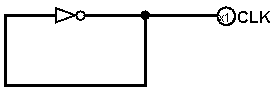
A simple clock, which would be classified as a "relaxation oscillator"
"What the fuck is this?" you might ask. Remember that it takes time for logic gates to generate output, and it takes time for that output to propagate back to the input; the result of this is that CLK will fluctuate between High and Low with a (relatively) steady rate, making it an oscillator.
Most of the time the delay between the two gates will be different so that the whole circuit will eventually settle down to either Q=1/NEG_Q=0 or Q=0/NEG_Q=1 - but we can't predict which state we will be in. This is not desirable for a storage device, so we have to find ways to fix this.
Gated Set-Reset Latches
The output state of the SR latch presented above is directly linked to its inputs (which in some texts called "transparent"). Sometimes this is kinda messy to handle, so people added an Enable signal to control when will the S and R signal have their effects.
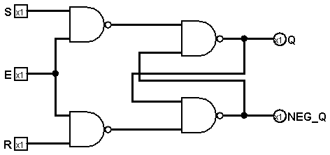
Gated SR latch built with NAND gates. Note that it's *S* and *R* now because we use NAND gates so the thing (?) gets inversed.
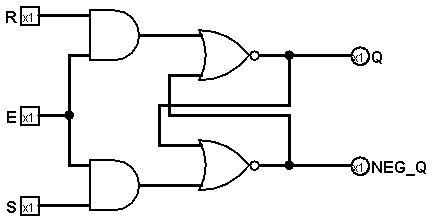
SR latch built with NOR and /AND/ gates.
This does not fix the oscillating problem though.
(Gated) D Latches
The two useful input combination of an SR latch is R=0/S=1 and R=1/S=0 from which we can conclude S=~R (or R=~S), thus we can combine the two signal into one, called the Data signal:
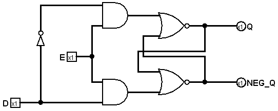
D latch built with NOR, AND and NOT gates.
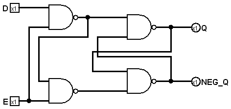
D latch built with NAND gates. This is kinda tricky to explain: when E=1, the gate near D works effectively as an NOT gate so we can take the inverted D for R from there, and when E=0 the original SR latch part will have an input of NEG_S=1/NEG_R=1 which is S=0/R=0, which is the "latch" state.
This fixes the oscillating problem because S=1/R=1 simply can't exist with this configuration.
D flip-flops
In case of terminology, the difference between latches and flip-flops seems to be how the change of Q is triggered: latches are level-triggered, which means the change of Q is triggered by the change of the level of input; flip-flops are edge-triggered, which means they take a CLocK signal and Q changes on the time when this signal change, i.e. the edge of (the CLK signal) level. Edge-triggered flip-flops can be divided into rising-edge-triggered and falling-edge-triggered, but the basic principle is the same - you can just put a NOT gate in front of the CLK signal to convert one to another.
The simplest D flip-flop can be constructed with two D latches; this is called the Master-Slave D flip-flop:
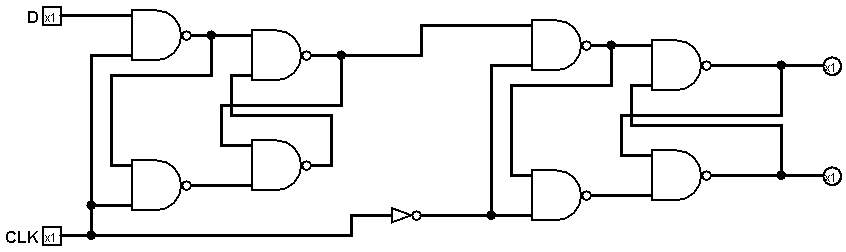
Master-Slave D flip-flop.
The idea behind this is the first latch propagates D to the D signal of the second latch when CLK=1, and the second latch propagates that signal to Q when CLK=0 and thus propagates D to Q when CLK goes from 1 to 0, i.e. falling-edge. (note that the E signal of the second latch is connected with a NOT gate.) Put a NOT gate at the very beginning of the CLK signal and you'll get a rising-edge D flip-flop.
The most common usage for D flip-flops is probably shift registers, which is a core part of serial and parallel interfaces.
SR flip-flops
Here comes the third bit of confusion: SR latches (level-triggered) are sometimes called SR flip-flops (edge-triggered) as well. To make this flip-flop is easy though - return the D signal into S and R from the D flip-flop and you're done:
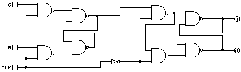
Falling-edge-triggered SR flip-flop.
JK flip-flops
I don't know why it's called JK flip-flop, but basically it's a SR flip-flop that when it's put in the "invalid" state of R=1/S=1, instead of making Q=NEG_Q=1 it toggles Q.
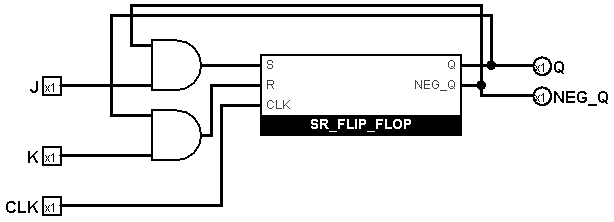
JK flip-flop.
This is fairly easy to understand. AND gates are added, so:
- K=1 is only allowed to propagate into R when Q=1/NEG_Q=0, which means "only when the bit is set can this bit be reset".
- J=1 is only allowed to propagate into S when Q=0/NEG_Q=1, which means "only when the bit is unset can this bit be set".
- When K=1 and J=1, Q and NEG_Q are propagated back to R and S respectively, turning Q=1/NEG_Q=0 into R=1 and thus resetting Q, or turning Q=0/NEG_Q=1 into S=1 and thus setting Q. Remember there's gate delay, so it takes time for the propagated Q/NEG_Q to feed through the internal SR flip-flop and generates a new state.
T flip-flops
T flip-flops are simply JK flip-flops with J=K; this means the Q signal of a T flip-flop can only stay or keep toggling. The frequency of Q toggling is half the frequency of the CLK signal, which is very handly for making counters.
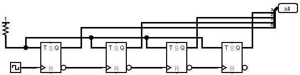
A basic 4-bit counter with T flip-flop.